-
• #27
If you're going to put it up for sale somewhere, you should do a few project on it too. With side by side 'normal' and yours. Far too often I see some board and I go "how would this help me" / "show me an implementation".
It's not that I can't with this particular board, but I think it's a good idea never the less.
Show us some photos when you get them please :)
-
• #28
AWW YA!
Scheduled Delivery:
Today by End of DayFriday, April 17, 2015 Location Time
17 With delivery courier BOSTON, MA - USA 10:26Yeah - I'm definitely going to do a project or two on it and put it up.
-
• #29
I had the WIZnet PCBs done in 0.8mm. Not sure why now.
Anyway, it actually seems quite good. A little flexible (I guess you wouldn't want big parts on it), but good enough. I'm not sure about the Protoboard, but it'd be great for most of the shims.
-
• #30
I think I got some wiznet adapters with my pledge - that means I should be getting wiznet PCBs in my shipment right?
Sweet, I can take a pair of scissors to them and see how well 0.8mm PCB cuts....
-
• #31
Should be... I think 0.8mm PCB would blunt scissors pretty quickly - I'm interested to see though!
-
• #32
Good catch! I'll use my roommate's scissors. :-P
-
• #33
Got my protoboards today!
Found a few problems:
USB cutout needs a wee bit more space
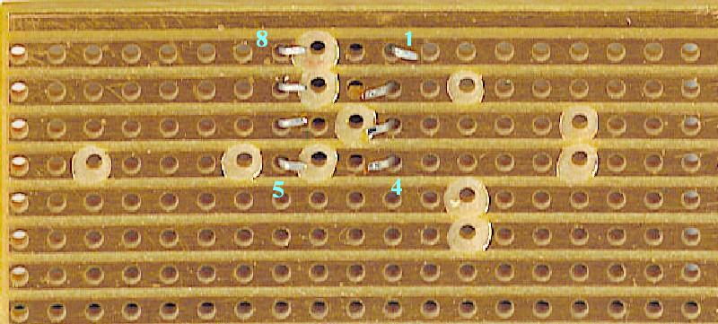
Vcc and Ground exposed traces shortedSplitting the 4's up into pairs of 2's did NOT work. Turns out even without the solder mask, it's hard to join the pads (same as if there was solder mask) with a blob of solder - and in the process of soldering in the Espruino, you'll almost unavoidably plug up the holes if you're using the castelated pads. So yeah, that's a no-go, going back to rows of 4. Unfortunately, this kills the use of this version with the castellated pads, because you block up all the holes that the pins are connected to! (This is what prototypes are for). I'll try another design for split headers....
0.8mm cuts with scissors. I don't think it's good for them, but it cuts okay.
In any event, this batch isn't going on ebay. Not eBay grade. Contact me if you want some protoboard protos.
-
• #34

I'm gonna try more aggressive pad shapes in some of my next prototypes, I was really hoping I'd be able to bridge the adjacent pads if I tried - but I can get solder all over every hole in a 3 hole radius without bridging anything with this layout :-P
5050 pads need to be larger to facilitate soldering on those leadless bastards.
TSSOP pads need to be longer to accomodate smaller TSSOP sizes comfortably.
All the other part outlines look good.
I'm gonna move the SOT-89's around, and see if I can fit an uSD card holder outline there ;-)
And uh, there's a little problem with using 0.1" and 0.05" pin headers to mount the Espruino removably on a board, barely worth even mentioning...

Yeah, the 0.05"'s are shorter, so you'd need to scare up extra long 0.05" header.
On the plus side, I think they'll be mostly used as castellated pads, which they excel at. A true joy to solder in, particularly with a touch of no-clean gel flux.
Other changes:
Replacing MSOP-8 pads with MSOP-12 (no idea if that's a thing, but more space with those pads - there was space, and traces that were easy to get at.
Going to try to clean up the power area and see if I can make room for silks.
Overall, pretty happy. The mondo downer is the difficulty of bridging traces intentionally.
-
• #35
There was a time where the heart of a board - cpu - was the center of attention. With Pico it looks like the heart fits like a header / connector / socket, and everything else gets the day in court.
0.05" headers look like a bit pity... understandably: why would you make them as tall/long as the 0.1", because you just shrunk the pitch to 50%... so the 0.05" option in combination with 0.1" headers may not have been the most thought through decision... but may be this start the 'revolution' to do everything in 0.05" pitch, including bread boarding, the way the 0.1" pitch is established. Of course, I would then need to use my desk magnifier glass all the times... ;-)
-
• #36
Replace split 4's with 4's *done
Lengthen pads on TSSOP and 5050, retrack appropriately. *done
Replace MSOP8 with MSOP12 *done
Fix short between power and ground strips *done
Fix mill dimensions around mini USB, fit an extra row of 4 holes *done
Fix extra solder mask on bottom *done
Make gap in ground for a mounting hole *doneI don't think I have space for the micro SD card. Will have to try again tomorrow.
Not sure what to do w/regards to the desire to mount the Espruino so it doesn't overhang. The bit about the pins , and having to chew out a half inch by half inch chunk of PCB to fit the mini USB connector if you do it surface mounted.. I think that dream may be dead.
Still to do is cleaning up power area, and getting some markings in, and fitting the third mounting hole, if I can find somewhere for it.
I wonder if I can draw in negative on the solder mask, and thus mark ontop of the otherwise exposed traces. I wonder if that would even come out. Otherwise, I may mask off a short section of the ground/power traces in a few places so I can put a label on the silk. -
• #37
Sorry to hear the 2x2 didn't work (apologies for the idea). Maybe you could drill a hole in the middle so one could use one of those perfboard tools that twists the track to cut it?
So one could do this:
Looks good!
-
• #39

Mounting holes. All grounded.
Expanded TSSOP and 5050 pads.
Silkscreen labels on pads broken out from Espruino
Silkscreen labels on power stripes and regulator outputs.Added spot for electrolytic cap on input.
Added breakout for Enable pin on the SOT-23-5 regulator (oops)
Added spot for a 1210 cap on the ESP8266, since they seem to need a really beefy cap on supply. Caps are available up to 100uf in that size, which should be more than enough! -
• #40
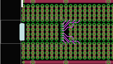
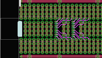
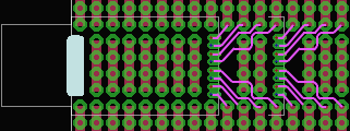
Did you ever think a bit in the direction(s) the attachments convey? @DrAzzy, your work got me - may be a bit too - excited... ;-). @Gordon, could that be some shim - and even carrier / breakout - ideas as well? ...because It would bring the connectivity into just 2 single, parallel rows... (I 'accepted' the perpendicular rows - in the first place - only because they yielded to a smaller size, even on the standard board...).
For the not overhanging placement on @DrAzzy's proto-board and and its derived carrier board, a pin headers can be soldered between the Pico and the board for 'distancers' to give enough clearance for the cable to plug or (micro?) USB socket to mount. The headers can also be replaced by just wires, as @Gorden shows for attaching the already available shim. I'm not to much worried about the extra height this adds.
The (thin) shims can be soldered on either bottom or top of Pico, and with thin shims, two pin headers can be soldered across Pico and the shim along the long edges to give the overal board the typical two-row pin header look and application options.
With some
PS: regarding the routing: my experience in that matter is quite outdated, so it may be a bit far (tight) fetched... on the other hand that @Gorden made the routing in regard to the 0.05" pin row makes it look feasible to me.
5 Attachments
-
• #41
Yes, I think a 0.1" 'breakout' shim could work really well. There's obviously still the issue of height (and also leverage!) but maybe a shim that went right along the board and added pins to the edge would work well and would be strong too.
-
• #42
I'll see what I can do with tracking that. That block of 9-wide through-hole near the FETs might be another option - maybe it could be reversed, and 2 row-2's added for A5/A8, or something like that....
Anyone got any thoughts on the revised design?
I'm going to send that out for Rev. A early this week I hope, along with a couple of related designs, and a test pattern with the (hopefully) bridgable rows, holes that are easy to bridge with the exposed ground/power traces, etc
-
• #43
I think I've gotten it figured out for the second positioning of the Pico
The 8 2-rows currently connected to 0.05" header are removed. The first 0.05" header goes to the next 4 rows of 4 along the outside.
The next row of 0.05" header is lined up with the fourth row of holes on either side (ie, the last one connected to the first 0.05" header. Beyond this (moving towards the right of the board), the next two rows of 4 in the middle are gone, and the third replaced with two rows of 2. The 0.05" header in the second row is wired to the next three rows of header in the outside, with the middle two pins going to the two rows of 2 in the middle (this gives you one more row of holes).a DIP20 can still be fit, but you need to use the DIP area on the top right, below the fets, for it, and you use two lines of the interfacing area. But how many people are going to be using 2mm or 0.05" pin header on the right - and need two blocks of it, and a DIP-20?
The plan is for an order to go out to our dirty hookup in the east by the end of the week with this and some generic and AVR-friendly protoboards.
-
• #44

-
• #45
Wow, looks neat!
Just a thought, but if you also put a third row of 0.05" right next to the one in the middle of the board (and connected to the first row), you could also use it as a break-out for 0.05" dual row header.
-
• #46
Neat and very safe solution - the routing from 0.05" rows to 0.10" left and right sideline rows. The few holes that have to be given up don't make a dent at all.
For a shim it looks a bit different: having even one row more: a 2 x 14 = 28 wide DIP resembling solution adds at the same time already a minimal proto board - even more with castellations:
1 Attachment
-
• #47
@allObjects I'm not sure what you're talking about here, frankly.
- What do you mean "for a shim" in this context?
- Where are you saying a DIP-28 could fit?! We're not even close to being able to fit one in the throughhole area around the Pico.
- You can't run a trace through an area that has exposed copper on both top and bottom, and I don't think i can track between the holes at all. Those prototyping rows have larger pads around the vias than normal.
- What do you mean "for a shim" in this context?
-
• #48
Going to pull the trigger on Rev. A shortly.
-
• #49
DrAzzy, The work you’ve put into this board is nothing short of amazing. With the fix to power busses and through-hole size I believe this is one the best prototyping board out there. There are not square vias, but just in case, if you could put some square soldering pads on through-holes which could possibly indicate the pin 1 of any IC. You can place those after 10 or 20 vias in a line so that people can use those to indicate the first pin of their ICs.
-
• #50
Uh, and where exactly would those go?
Even if I put them on the SOIC-16, there are perfectly good reasons to not put your SOIC part lined up with the end (for example, if you're using one of the LEDs that shares the pins with the pin that would normally be pin 1). Or you may put several IC's next to eachother.
I don't see how I could do this without a project made on the board inevitably ending up with square holes on pins that aren't pin 1, and non-square holes on pins that are - in which case the decoys are probably worse than having nothing, because they'd be lying to you more often than they told the truth.
 alexanderbrevig
 DrAzzy
 Gordon
 allObjects


 caliskan
Should be arriving by DHL, either today or next delivery day (i don't know which days DHL does).
Osterle: SMD stuff pops right off flexible PCB, and even ignoring that, the flexing due to vibration makes things made with it less reliable. I've used flexible PCB with SMD components, and it had failed within hours due to normal vibrations within only 3 hours (lasted just long enough though.).
I'd love to make the stuff easier to cut though - I wonder if I could just use slightly thinner PCB than usual. I went with 1.6, but maybe I should go 1.2 or even less, in the interest of making it easier to cut. I'll get some trials in other thicknesses when I place my next order. I'll try cutting it with a variety of implements.